|
|
|
An introduction to
EBSD
Backscatter Kikuchi Diffraction
in the Scanning Electron Microscope

("BKD", "ACOM/SEM",
"Orientation Microscopy")
Prof. Dr. Robert Schwarzer
Kappstr. 65
D-71083 Herrenberg
Germany
E-mail: mail@ebsd.info
Revised December 12, 2024
|
Abstract
This web site provides a short introduction to Automated Crystal Orientation Microscopy (ACOM), a technique based on Backscatter Kikuchi Diffraction (BKD) in the Scanning Electron Microscope (SEM).
The technique is often called Electron BackScatter Diffraction (EBSD), in particular when referring to automated commercial systems. However, the acronym "EBSD" or similar abbreviations should not be mistaken for Backscatter Electron Diffraction (BED) in general. Backscatter electron diffraction from bulk surfaces comprises four well-established techniques:
• Low Energy Electron Diffraction (LEED)
• Reflection High Energy Electron Diffraction (RHEED)
• Backscatter Channeling Diffraction (ECP)
• Backscatter Kikuchi Diffraction (BKD, EBSD).
EBSD has become very popular in materials science and geology during the last decade. There are several reasons for the success of this novel technique:
• A wealth of information is obtained about the crystallography and microstructure of bulk polycrystals.
• The importance of crystal texture and materials' anisotropy has been generally realized.
• Progress in low-light level camera and computer technology has enabled fast and automated systems.
• Commercial systems are easy to operate.
• Specimen preparation is relatively simple.
• Scanning electron microscopes are widely available in many laboratories.
Download  Overview: Backscatter and transmission
Kikuchi diffraction for materials science. Overview: Backscatter and transmission
Kikuchi diffraction for materials science.
History of EBSD
|
1928
|
Shoji Nishikawa
and Seishi Kikuchi
The
Diffraction of Cathode Rays by Calcite.
Proc. Imperial Academy (of Japan) 4 (1928) 475-477, with 2 figures
The first EBSP was published by S. Kikuchi and S. Nishikawa, his supervisor, in 1928, as a compliment to Kikuchi's papers, he had published several pages before in the same volume, on similar patterns obtained in a transmission experiment on mica foils. They
directed a beam of 50 keV electrons from a gas discharge on a cleavage
face of calcite at a grazing incidence of 6°. Diffraction patterns were
recorded on photographic plates placed 6.4 cm behind the crystal, normal
to the primary beam. The patterns consisted of pairs of parallel black and
white lines, and in some cases contained diffraction spots in addition.
When the photographic plates were placed in front of the specimen
(parallel with the primary beam, as nowadays in modern "EBSD" set
ups), the same type of pattern was observed as well "which must have
been produced by the electrons deflected through an angle greater than 90°". Since transmission and backscatter patterns were quite similar, they
have been likewise interpreted and indexed. The relative intensities of
high-order reflections were compared with those of X-ray diffraction.
Cleavage faces of mica, topaz, zincblende and a natural face of quartz
were also tried, and it was found that they give similar backscatter
patterns.
|
|
")  The
authors called this new type of pattern "P-pattern" or "pattern of
the fourth kind" (= "black and white lines in pairs due to
multiple scattering and selective reflection"). They have later
been named "transmission Kikuchi patterns" respectively "
reflection Kikuchi patterns" or "backscatter Kikuchi patterns". The
authors called this new type of pattern "P-pattern" or "pattern of
the fourth kind" (= "black and white lines in pairs due to
multiple scattering and selective reflection"). They have later
been named "transmission Kikuchi patterns" respectively "
reflection Kikuchi patterns" or "backscatter Kikuchi patterns".
The low quality of the first BKP may be caused by specimen contamination
due to the poor vacuum facilities at that time.
|
|
Shoji Nishikawa and Seishi Kikuchi
Diffraction of Cathode Rays by Calcite.
Nature 122 (1928) 726
A short communication in Nature appeared at the end of the same year in which
Nishikawa and Kikuchi already reported the main features of BKP (bands
bordered by parallel lines at a width of twice the Bragg angle; high-order
reflections; center line corresponding to the section line of the lattice
plane with the screen; intensity approximately predicted by the structure
factor; wide-angle diffraction). In the outlook they anticipate that
the above mentioned backscatter method [today known as EBSD] would be more
useful than the transmission method on account of its possibility of
extensive application on many crystals...
Seishi Kikuchi
Beugung der Materiestrahlen.
Physikalische Zeitschrift 31 (1930) 777-791
S. Kikuchi gives a review of electron and ion diffraction, at that time, by single crystals, gases and molecules. He states that the intensity profile of the (today named) Kikuchi bands is not explained by the simple kinematic theory. His focus is on the Mean Inner Potential and the Atom Form Factors for structure analysis.
In the following publications Seishi
Kikuchi and Shigeo Nakagawa concentrated their studies on the deviation of
the lines from the exact Bragg position caused by anomalous dispersion of
crossing lines and the effect of the refractive index of the lattice on
fast electrons.
S. Kikuchi and Sh.
Nakagawa
On the reflection of cathode rays from single crystal surfaces. (paper
in German)
Sc. Pap. Inst. Phys. Chem. Res. 21 (1933) 80-91
S. Kikuchi and Sh. Nakagawa
The anomalous reflection of fast electrons from single crystal
surfaces. (paper in German)
Sc. Pap. Inst. Phys. Chem. Res. 21 (1933) 256-265
Already in 1928, Seishi Kikuchi
(August 25, 1902 - November 12, 1974) grew fond
of atomic physics. He published an investigation on the mode of
disintegration of Radium (J. J. Phys. 4(1928) 143), made the acquaintance of
Werner von Heisenberg on his visit to Japan, and joined for some time
Heisenberg's team at the university of Leipzig (Germany). Back in Japan,
starting in 1934 he installed a 600 kV Cockroft-Walton high-voltage
generator, the most powerful at that time, and a charged particle
accelerator at the (now) Osaka University Physical Science Department.
Seishi Kikuchi is known as an outstanding Japanese nuclear physicist.
|
|
1932/33
|
K. Shinohara
Diffraction of cathode rays by single crystals. Part III.
Sc. Pap. Inst. Phys. Chem. Res. 20 (1932/33) 39-51 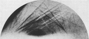
Kikuchi envelops are reported in
backscatter Kikuchi patterns from cleaved calcspar (calcite, CaCO3)
at 44 keV.
|
|
1933
|
R. von Meibom and
E. Rupp
Wide-angle electron diffraction. (paper in German)
Zeitschrift für Physik 82 (1933) 690-696
In backscatter diffraction of fast electrons from rocksalt, sylvine,
fluorspar, diamond, calcspar and quartz crystals, dark bands (on the
photographic negative) have been reported that are bordered on both sides
by (Kikuchi) lines. The bands were visible through acceptance angles up to
160°. The angle of beam incidence was varied between 3° and 30°, the beam
voltage from 10 kV to 40 kV. The band width is proportional to 1/d (d = lattice spacing).
Intensity profiles across two typical bands are sketched. Experiment
showed that the bands are formed by backscattered electrons of virtually
the same energy as the primary beam energy. The center lines of the bands
- now called Kikuchi bands - have been indexed as zone circles sectioning
the cylindrical recording film.
|
|
1937
|
H. Boersch
About bands in electron diffraction. (paper in German)
Physikalische Zeitschrift 38 (1937) 1000-1004 and image table XI
The identical publication also appeared in: Zeitschr. f. techn. Physik 18 (1937) 574-578 and image table XVI
Boersch studied thoroughly - in addition to transmission - also backscatter Kikuchi patterns (at 20 kV, about 5° of incidence and up to
162° of acceptance angle) obtained from cleaved, polished respectively
etched NaCl, KCl, PbS, CaCO3,
CaF2, quartz, mica,
diamond, Cu and Fe surfaces.
|
|
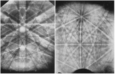
Backscatter Kikuchi patterns obtained
from iron (left) and fluorspar (fluorite) (right),
recorded on a cylindrical film at 20 kV.
|
|
Boersch used flat photographic plates
as well as a cylindrical specimen chamber with a cylindrical film to
record high-angle Kikuchi patterns. The angular range is considerably
larger than that obtained before in the TEM and in present SEM appliances.
The patterns are remarkably sharp and rich in detail. The widths of the
bands was found, in agreement with Bragg's law, to be related to the
energy of the incident beam and the interplanar lattice spacings.
Boersch has discussed the origin of
Kikuchi lines, dark and bright bands and envelops taking von Laue's
dynamical theory of electron diffraction into consideration.
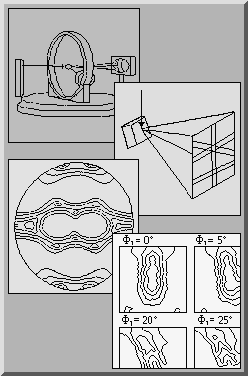
G.I. Finch and H.
Wilman
The study of surface structures by electron diffraction.
Ergebnisse der exakten Naturwissenschaften 16 (1937)
353-436
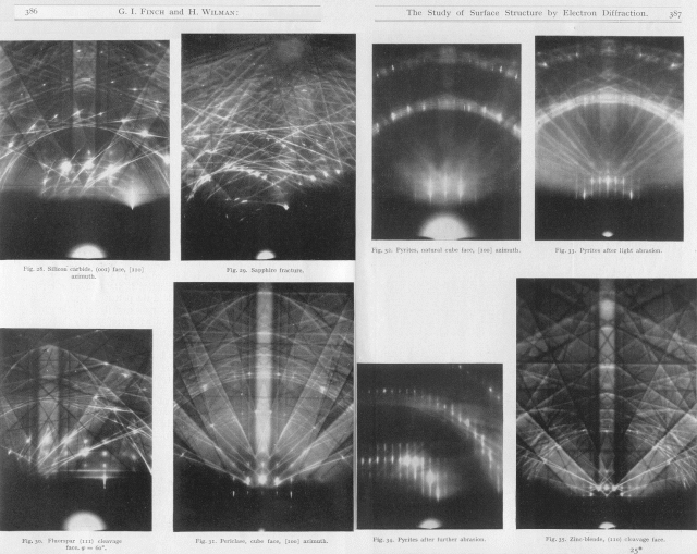
In this review a collection of excellent backscatter Kikuchi patterns form
a variety of single crystal cleavage faces have been presented.
|
|
1944 and 1948
|
Max von Laue
Materiewellen und ihre Interferenzen.
Akademische Verlagsgesellschaft Geest & Portig K. G., Leipzig 19
44; reprint 1948
The intensity pattern outside a crystal due to a point source of charged
particles inside the crystal was quantitatively explained by von Laue when
he solved the problem of bands in patterns as observed by S. Kikuchi. Many
examples of observed patterns and the theoretical development can be found
in his book "Particle Waves and Their Interferences" (in German). After electrons are inelastically scattered the original spherical
wave is considered as a superposition of several Bloch waves inside the
crystal, taking appropriate boundary conditions at the crystal surface and
absorption by imaginary structure potentials into account to determine the
intensity pattern outside.
|
|
1947, 1948
|
K. Artmann
On the theory of Kikuchi envelops. (paper in German)
Zeitschrift für Physik 124 (1947) 80-104, 154-174; 125 (1948)
27-58, 298-335
The formation of Kikuchi envelops is treated without using the reciprocity
law as well as in a rigorous wave-dynamical treatment based on the
reciprocity law, a one dimensional and a three dimensional periodic
crystal lattice. A good agreement of both features, surface lattice
envelops and crystal lattice envelops, with experimental findings has been
obtained.
(Remark: Kikuchi envelops can
have a ring shape or a parabolic appearance. Perhaps due to the similarity
with HOLZ rings of spots in transmission electron diffraction on thin
foils, the ring shaped envelops are sometimes named "HOLZ lines"
in recent publications even in the case of BKD. One should, however, bear
in mind that Kikuchi envelops are definitively an effect of dynamical
rather than kinematical diffraction. The Ewald construction is a very
useful model for illustrating the formation of diffraction spots, but it
is not applicable to BKD. In particular, there is no coherence between a
primary beam and the diffracted beams.)
K. Artmann
On the theory of Kikuchi bands. (paper in German)
Zeitschrift für Physik 125 (1948) 225-249
The formation of Kikuchi patterns is treated by using the reciprocity law
and solving the Schrödinger equation for bound electrons in the three
dimensional crystal potential. This approach of dynamical theory of
electron diffraction leads to a good agreement of the intensity profile
and location of Kikuchi bands with experimental results.
|
|
|
Kossel patterns in
X-ray diffraction closely
correspond to Kikuchi patterns in electron diffraction. If they are
generated with hard X-rays of, for instance, higher than 100 keV energy
when X-ray wavelengths are in the range of the wavelengths of electrons in
the SEM, the Kossel cones degenerate into almost straight lines so that
these Kossel patterns look very similar to Kikuchi patterns.
"Download H.
Determann
Kikuchi-Bänder mit Röntgenstrahlen. (in German with
attached English translation)
Schriften der Naturforschenden Gesellschaft in Danzig 1938, pp. 5-7
H.C. Wolf:
Gitterquell-Interferenzen harter Röntgen-Bremsstrahlung. (in
German).
Annalen der Physik 448 (1953) 381-403
Diffraction of ions, such as protons
or He+, by single crystals can as well generate patterns very
similar to Kikuchi patterns. They are known as Ion Blocking
Patterns.
For details visit www.crystaltexture.com
|
|
|
...... many publications have appeared since then, for example:
|
|
1954
|
M.N. Alam, M. Blackman and D.W.
Pashley
High-angle Kikuchi patterns.
Proceedings of the Royal Society of London A 221 (1954)
224-242
A
cylindrical specimen chamber and camera have been used to study high-angle Kikuchi patterns obtained by reflection of electrons, of energy
6 to 50 keV, from the cleavage surfaces of crystals with the sodium
chloride structure. Angles of scattering ranging from 0° to 164° were
covered. The relative intensity of the patterns at different scattering
angles was measured using a photographic technique. The intensity
distribution was found to become less steep as the energy of the incident
electrons decreased. In photographs taken with a large value of the
glancing angle of incidence, defect bands were found, starting near the
shadow edge of the pattern. These changed to excess bands at higher angles
of scattering.
The most striking feature of the results is the remarkable intensity and
clarity at the highest scattering angles of the patterns produced by
crystals such as lead sulphide and potassium iodide, the constituents of
which have a relatively high elastic scattering cross-section. In marked
contrast, a relatively low intensity and low clarity was found at these
angles for lithium fluoride under the same experimental conditions. An
investigation of the width of Kikuchi bands, visible over the whole
available angular range, showed that the electrons forming these bands had
the same energy as that of the incident electrons within the experimental
error of 10%. A possible mechanism is discussed by means of which
electrons can be diffused through large angles with high efficiency,
relative to small angles, and with relatively little loss of energy.
In essence, the findings of H. Boersch (1937, see above) have been confirmed.
|
|
1973
|
J.A. Venables, C.J.
Harland
Video camera attached to the SEM. They have coined the new term "EBSP" (= Electron BackScatter Patterns) for backscatter Kikuchi patterns.
|
|
1987
|
D. Dingley & Link: 1st commercial system for the SEM
The user had to identify and locate 3 zone axes on the screen, then
the program calculated the rotation matrix; feasible for cubic crystal
symmetry.
|
|
1990
|
N.-H. Schmidt (Risø; HKL): commercial system ("Channel")
The user had to mark interactively 3 or more bands to automatically index the pattern.
|
|
1992
|
N. Krieger Lassen, D. Juul Jensen, K.
Conradsen
Automated indexing using the Hough transform and a butterfly mask
|
|
1993
|
B.L. Adams, S.I.
Wright
"OIM": mechanical stage scan; Burns algorithm, Hough transform.
|
|
1994
|
Niels Krieger Lassen (PhD Thesis at Risø and Univ. Lingby, Denmark)
Thorough investigation of the Hough transform for automated EBSD.
|
Some of our contributions
|
1989
|
(Peltier cooled) CCD
camera employed for BKD
|
|
1993
|
Intensified CCD camera, interactive measurement of BKD band positions with the cursor on the monitor screen, automated indexing and orientation calculation.
Modified ORKID/TEM version, supports all
crystal symmetries.
|
|
1994
|
Digital beam scan for
automated BKD
|
|
1997
|
ACOM (ORKID/SEM)
The SEM is operated under full control of ACOM software:
. dynamic focusing and dynamic system calibration,
. automatic setup calibration,
. all working distances and magnifications of the SEM are available
for ACOM,
. automatic acquisition of flat images,
. Radon transform (RT) for automated extraction of band positions, no butterfly mask is used,
. Pattern quality computed from RT and
1D FFT.
|
|
1998
|
Iterative refinement of the scanning
grid ("mesh refinement")
|
|
2001
|
Pattern solving by the combination of Radon
Transform with Artificial
Neural Networks
(ANN, artificial intelligence)
|
|
2007
|
Fast EBSD in cooperation with Prof. Dr.
Jarle Hjelen, Trondheim
|
|
2009
|
EBSD detector employed as a multi-array
detector to construct microstructure images which reveal topographic,
material Z as well as lattice directional contrast during the acquisition
of pattern sequences on-line or off-line in FastEBSD (see
Poster Kiel 2011 ).
|
|