|
| EBSD and BKD |
|
|
|
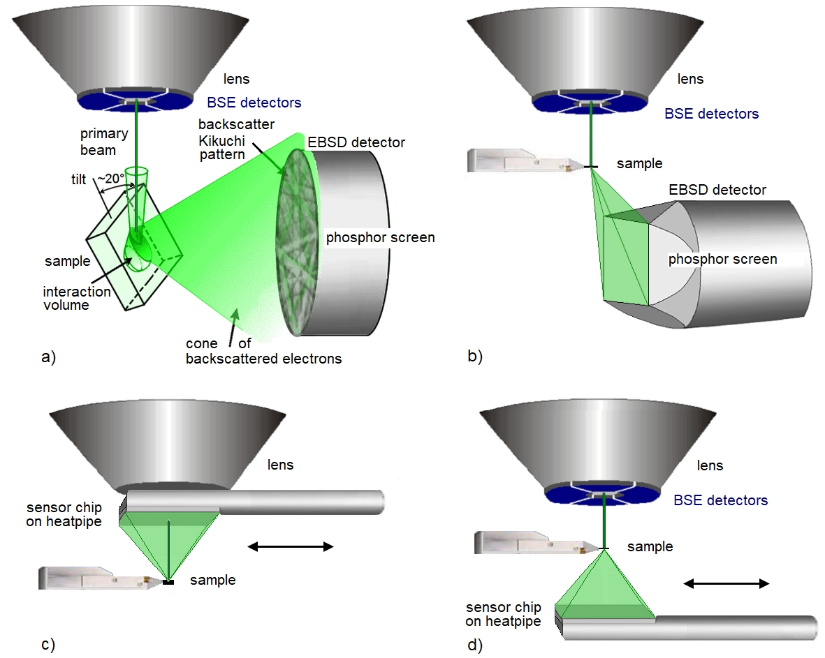
Acquiring Kikuchi patterns in the SEM In conventional EBSD mode, the sample surface is steeply tilted by 60°-70º from the horizontal with respect to the primary beam (Figure 1a). This tilt is undesirable but necessary to produce a Kikuchi pattern of sufficient intensity, due to the strong forward scattering of high-energy electrons. As a consequence, a steep intensity lobe is generated. Its maximum is close to the direction of optical reflection that a light beam would haveon an opaque surface. The EBSD detector is set up horizontally on a retractable stage on a side wall of the specimen chamber. The height of the EBSD detector is therefore set such that the intensity maximum falls on the center of the phosphor screen. The distance between sample and screen is typically 2 cm, which corresponds approximately to the diameter of the screen. A wide cone of about 45º of backscattered electrons is detected. The backscattered Kikuchi pattern/image is usually projected onto a phosphor screen. A thin coating layer of aluminum is often applied to increase the brightness of the phosphor by reflecting the light back to the camera. It also acts as a passive energy filter by absorbing low-energy electrons. The most important function of the coating is to ground the phosphor screen. The images are captured with a low-light CCD or CMOS camera (indirect detection) (Fig. 1a, b). The speed and sensitivity of CCD cameras are improved by grouping neighboring pixels into "super pixels", a procedure known as "binning", but at the expense of resolution. For phase identification and internal stress analysis, for example, high-quality EBSD patterns are captured as complete images (without binning). Time-averaging techniques are used to reduce noise and achieve sufficient intensity. Direct pixelated detectors lead to a significant improvement in detective quantum efficiency. Sensors are currently being developed [1-6]. The pixelated detector converts the collected electrons directly into intensity data, with low noise and improved quantum efficiency.The detector is mounted concentrically to the primary beam spot either above (Fig. 1c for BKD) or below (Fig. 1d for TKD) the sample which is in a horizontal position at a slight tilt angle [5, 6] to improve spatial resolution and electron channeling contrast imaging (ECCI). The undesirable side effects of a steep sample tilt (reduced spatial resolution, distortions of the pattern and raster scan) are avoided. The use of multi-array image detection eliminates the need for additional BSE detectors. Currently, the speed exceeds several thousand images per second [1].
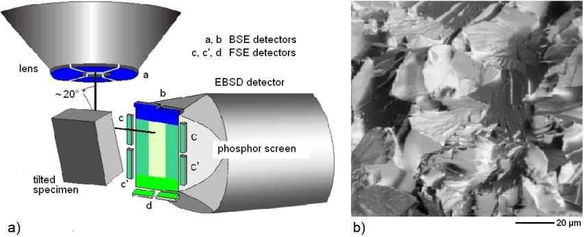
Figure 1 Kikuchi diffraction in the SEM. The conical sections of the recorded patterns are marked in green. Indirect detection uses a phosphor screen optically coupled to a CCD or CMOS camera. Fig. 1a shows the BKD setup with tilted sample. In TKD, a standard EBSD detector comes from the side below the horizontal sample (Fig. 1b) and captures about half of the cone of transmitted electrons. The recorded image sequence is digitized, transferred to a PC, corrected for background noise, indexed online or stored permanently for later analysis. Digital beam scanning is preferred for orientation mapping as it has a higher speed compared to mechanical scanning of the stage. The steep inclination of the sample has unwanted side effects on digital scanning systems, as the diffraction geometry changes from one measured point to the next, and the beam spot becomes blurred as the sample is scanned down line by line. Consequently, the distance between the sample and the screen and the center of the image must be automatically calibrated from one scan point to the next, and the electron probe's forming lens must be dynamically focused. High spatial resolution can be achieved with correct focus settings, even at low magnification. In this way, a large sample area can be studied by coupling a mechanical stage and digital beam scanning. The microscope is thus under the full control of the EBSD program during the automated measurement. ______________ A fast EBSD System Our FastEBSD system consisted of a dedicated hardware detector NORDIF 1000UF and two separated programs which controlled the digital beam scan of the SEM as well as pattern store, off-line indexing and interpretation of the backscatter Kikuchi patterns (BKP). The patterns, after binning to 100x100 pixels on the sensor chip, were streamed on the hard disk as a sequence of bitmap images with 256 graytones to enable the access to the original raw data at any time. Some other EBSD systems relied only on reduced data sets such as Hough peaks. The detector contained a high sensitive CCD camera with GigE vision interface to the computer. Thus a high speed was obtained. GigE vision is an economic camera interface because no frame-grabber is required. The detector can be placed up to 100 m remote from the SEM. USB3 offers high speed at low costs as well. Some advantages of off-line over conventional on-line evaluation of the diffraction patterns are: Some further aspects of FastEBSD, in particular concerning combined analytical methods such as EBSD&EDS and EBSD&Phase-Sensitive Imaging, can be found on www.ebsd.de (in German). In 2015, when we terminated the FastEBSD project, the acquisition speed exceeded 1000 patterns per second. Speed of indexing pattern sequences was up to 2000 patterns per second on a PC. Since then, we have witnessed significant advancements in terms of both EBSD software and EBSD hardware (see section "Conclusions"). The Multi-Array Image Detector In scanning electron microscopy, backscattered electrons (BSE) can be used, as a complement to secondary electrons (SE), for imaging bulk sample surfaces. If the SEM sample is steeply tilted, as is the case for example in EBSD measurements to render subtle topographical contrast more visible, to reduce the penetration depth of the primaries, or to perform a Burgers vector analysis on dislocations, the usual BSE detectors on the bottom side of the probe-forming lens are ineffective. Therefore, special backscatter or forward scatter semiconductor diode detectors are occasionally employed, mounted for instance on the margins of the EBSD phosphor screen. [8]
Figure 2 a) The conventional BKD detector used as a pixelated multi-area detector. Optional solid-state BSE (marked in blue) and FSE (marked in yellow) detectors are no longer required. The EBSD detector by itself, however, can be used as a BSE detector for conventional imaging [9]. In our FastEBSD set-up acquisition boxes could be interactively set and (re-)adjusted on the phosphor screen by tracking with the mouse, at deliberately selected positions and sizes, to optimize contrast [10, 11]. In this way the EBSD detector was employed as a multi-array BSE image detector. High topographical and channeling contrast images and, if applicable, atomic number (Z) contrast images have so been obtained by evaluating streamed pattern sequences, depending on the sizes and positions of the acquisition boxes. Unlike special semiconductor detectors, the multi-array BSE detector does not further constrict the free space in front of the sample. The images are directly superposable and aligned to EBSD orientation maps and are so ideally suited to digital image processing. The technique is fast, convenient, and inexpensive. The topographic contrast can be well separated from the material contrast by setting the image boxes accordingly. In contrast to the construction of crystal orientation maps in the EBSD analysis of crystalline samples, the image sequences for BSE imaging do not have to be indexed. Therefore, BSE imaging with the EBSD multi-array detector is also suitable for non-crystalline materials [7, 12]. The next generation of multi-array EBSD detectors, especially those for direct electron detection, will allow fast sequences of several thousand frames per second, so that this method can be routinely applied not only for electron diffraction but also for general electron imaging in the SEM by replacing the usual Everhart-Thornley detector. __________ |

|
|